
Interconnect Defects in PCBs: Causes, Detection, and Impact on Reliability
Interconnect Defects
As circuit boards become ever more complex with multiple layers, finer lines, spaces and vias with smaller diameters, as well as greater aspect ratios, the possibility of an Interconnect Defect (ICD) looms large. If small hole voiding issues are not enough to keep everyone hopping, interconnect or interplane separation surely will. Unlike voids, whereby, if detected in time, the panels can be reprocessed, it is impossible to rework ICDs. Moreover, ICDs are not always detected by Quality Control.
The main reason is that ICDs are rarely caused by a catastrophic failure. Rather, constant thermal cycling or the high temperatures of assembly operations cause a weakened interconnect to separate. Many engineers expect that by performing one or two solder floats on plated coupons removed from panels will provide a sufficient QC check. Unfortunately, for the reasons cited above, this often allows the problem to go undetected, until it is much too late.
A slight separation can be detected after the coupon was subjected to two solder floats at 550° C for ten seconds. Generally, if not inspected by section, the panel would have easily passed electrical test. However, because of the weakness evident in the interconnect, continued thermal stresses and vibration of the PWB will most likely lead to an open. If in doubt about whether or not the defect is present, simply regrind and polish the potted coupon once again and inspect.
Remember, inspect for ICD only after polishing the coupon: do not etch the specimen. When a specimen is etched, a line of demarcation is often visible with electroless copper deposits. Such a line of demarcation may lead to concluding that it is a true ICD. It is imperative to use un-etched coupons to detect the presence or absence of the defect.
Certainly, an ICD is not confined to just the interplane. Blind vias can also exhibit a separation of the plated copper from the capture pad.
Interconnect defects (IP separation) generally exhibit these underlying characteristics:
• They occur during the stress of thermal shocks, such as soldering. This produces expansion in the Z-axis and places strain on the copper in the hole wall.
• They are most often seen on the first interlayer from either side of the board (i.e. in a 12-layer board, the defect is seen on the second and the eleventh layers).
• The weakest bond breaks first.
• Under cured boards are the most susceptible.
• They are affected by board construction - PWBs with more resin, less copper, lower Tg materials, tend to show more expansion in the Z-axis.
• ICDs are often (but not always) accompanied by hole wall pull away.
Interplane separation has many possible causes. This is what makes this defect so difficult to pinpoint and eliminate. And to confuse the issue further, there are three different types of IP separation:
• Type 1: Separation of the electroless copper deposit from the Interconnect.
• Type 2: Separation of the electrolytic copper deposit from the electroless copper deposit, with electroless copper remaining on the post.
• Type 3: Cohesive failure of the electroless, i.e. when the electroless copper deposit actually separates from itself.
The three types of IP failure (shown below) have their own inherent causes.
Type 1 Interconnect Defect
Type 1 ICD is the most common, and often the most difficult defect to troubleshoot, since it is affected by many process variables. Generally, there is significant internal stress of the electroless copper deposit. This stress causes the electroless copper deposit to pull away or separate from the interconnect post.
First, ensure that there is no drill smear remaining on the post: this might show as a separation, and lead to confuse smear with Type 1 ICD. However, the root cause is different. Type 1 ICD is caused by several factors, which may be interacting in such a way as to exacerbate the defect. Keep in mind that the weakest bond breaks first.
Generally, Type 1 ICDs can be attributed to the following:
• “Invisible” drill smear not removed by the desmear process. Check parameters if using alkaline permanganate or plasma. Is the drilling process creating more smear than normal due to dull drill bits, faster in-feed rates, poor quality entry and back-up material, or are drill bits remaining in-hole for an excessive amount of time?
• Micro-etch in the electroless copper pre-plate line not sufficiently “roughening” the copper surface to provide adequate anchoring sites for the copper deposit.
• Excessive dwell time in the catalyst or inadequate tin removal in the acceleration step; this leaves a “barrier” on the copper interconnect. Anything that weakens the bond between the copper deposit and the interconnect can be a cause for the separation.
• Drag-in of cleaners into the various process tanks or poor rinsing due to insufficient time, rinse water quantity or quality can cause Type 1 ICDs.
• Electroless copper deposit exhibits inherent stress; this is usually caused by the deposition rate being excessively high. The main cause of the stress is the amount of microinches of copper being deposited per minute. The process should be operated within the parameters that it was designed for. Any change in the process that causes electroless copper to be deposited at a higher-than-normal rate, will be sufficient to cause a Type 1 ICD.
A good rule to follow: if, for example, the electroless copper process is designed to deposit 40-50 microinches in 30 minutes, and the actual deposit is somewhere in the 70-100 microinch range, then there is a problem. The copper is being deposited much too fast. This will cause the grains of the copper to be “re-oriented.” This re-orientation leads to stress in the deposit; the only way for it to be relieved is for the deposit to pull away from the interconnect.
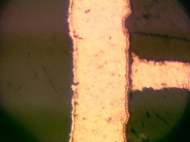
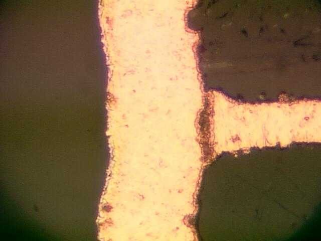
Type 2 Interconnect Defect
It is important to stress that Type 2 ICD is not an electroless copper/direct metallization/desmear problem. As shown in figure 2, the electroless deposit is firmly on the interconnect. The electrolytic copper has separated from the electroless copper.
Basically, the root cause of such a defect is lack of adhesion of the electrolytic copper to the electroless copper. When encountering this problem, the first order of business is to determine if the PWB was panel or pattern-plated. If pattern-plated, it is worth checking for develop or resist residues on the interconnect. Was the developer solution at proper concentration, temperature and pH? Is there resist lock in? These problems will prevent the electrolytic copper from adhering to the electroless.
Other potential sources of Type 2 defect are:
• Oxidation at the interconnect
• Poor adhesion of electroplated copper to the electroless
Oxidation is caused by long hold times between operations or rinsing with excessively hot water. In order to improve adhesion, a sufficient amount of copper must be micro etched. Typically, a 15-20 microinch etch is sufficient. Concern arises when only 10 or less microinches of copper are removed. This is generally an insufficient amount of copper removal to provide enough anchoring sites for the copper plate. Since many PWB fabricators have reduced electroless copper plating thicknesses to cut costs, they have been reluctant to be aggressive on the micro etch. The result is poor or insufficient anchoring of the electrolytic copper to the electroless. The solution to this problem is simple: if your electroless copper process cannot stand up to a microetch that removes 15-20 microinches, then find one that does!
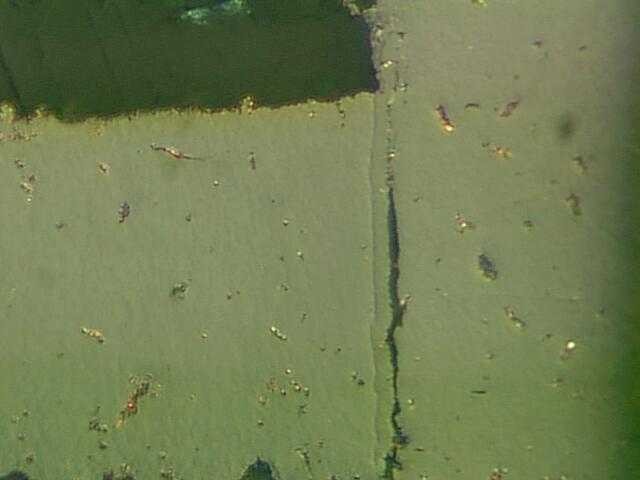
Type 3 Interconnect Defect
Type 3 ICD is a horse of a different color. Here, the electroless copper deposit actually separates from itself; this is known as cohesive failure. Basically, the copper is deposited in an unorderly fashion. Extreme deposition rates, over catalyzation, excessively high operating temperatures are all known causes of this type of ICD.
How Can Technic Help?
Technic has multiple solutions for your metallization requirements. If you want to reduce cost of operation, and, at the same time, improve its sustainability, Technic’s Circudep Black Knight is the ideal solution. This nano-dispersion of highly conductive graphite provides a wide operating window for the most complex PCB designs, including flex, rigid-flex, high layer count multilayer, and HDI/Ultra HDI substrates and packaging.
Black Knight provides a robust connection from the electrodeposited copper directly to the interconnect. Note that there is no electroless copper or catalyst layer acting as a barrier between the interconnect and the electroplated copper. As a result, there is no more robust connection between the post and the copper. IST and other thermal reliability test methods have confirmed the robustness of Black Knight. Sleep well at night. Call your Technic rep and get on board with Black Knight.
Author
.jpg) Mike Carano, PWB Final Finishes Consultant
Mike Carano, PWB Final Finishes Consultant
Add new comment