  • Applications
    • Semiconductor
      • Fabrication & Packaging Chemistry
        • Copper
        • Nickel & Tin
        • Precious Metals
        • Photoresist Strippers
        • Metal Etchants
        • Cleaners
      • Analytical Control (RTA)
      • Semiconductor Equipment
        • Semcon 1000
        • Semcon Fountain
        • Semcon 2000
        • Semcon 2500
        • Semcon Wafer Racks
      • High Purity Chemistry
    • Components, Lead Frames, Connectors
      • Electronic Component Chemistry
        • Connectors
          • - Precious Metals
          • - Non-precious Metals
          • - Post-Treatment
        • Lead Frames/LED Substrate Applications
        • Active & Passive Components
      • Electronic Component Finishing Equipment
    • Printed Circuit Boards
      • Chemistry
        • Photoresist Developers, Strippers
        • Preclean and Microetch Products
        • Desmear Chemistry
        • Metallization
        • Copper and Tin Plating
        • Final Finish - Electroplating
        • Final Finishes - Immersion
        • - ENIG
        • - ENEPIG
        • - EPIG
        • - ASIG
      • Imaging Products
        • Photoimageable Materials
          • - TechniFlex LCL
        • IRP Thermosetting Inks
        • Conductive Silver Paste
        • LED Inks
        • Peelable Masks
      • Process Control - EBA
      • Equipment
    • Industrial
      • Pretreatment
        • Cleaners
        • Activators
        • Etchants
      • Electrolytic Plating
        • Nickel
        • Tin
        • Silver
        • Copper
        • Zinc (EU Only)
      • Electroless Plating
      • Immersion
      • Post-Treatment
        • Anti-corrosion/discoloration coating
        • Anti Tarnish
        • Passivation
        • Coatings
        • Strippers
      • Industrial Equipment
      • Anodizing Equipment
    • Energy Technologies
      • Energy Technologies
        • Hydrogen Technology
      • Engineered Powder & Flake
    • Technic ECO Products
    • Decorative
      • Pretreatment
        • Soak Cleaners
        • Electrolytic Cleaners
        • Pickling Solutions
      • Plating Chemistry
        • Gold/Gold Alloy
        • Silver
        • Tin/Tin Alloy
        • White Bronze
        • Nickel/Nickel Alloy
        • Copper
        • Palladium/Palladium Alloy
        • Brass
      • Coatings & Coloring
        • Cataphoretic Lacquers
        • Color Treatments
      • Post-Treatment
      • Glass Etching
      • Equipment
    • Medical
      • Chemistry
      • Equipment
    • Application Support
      • Application Guides
      • Application Notes
  • Chemistry
  • Equipment
    • Automated Systems
      • Hoist Systems
        • Cantilever/Sidearm
        • Rail/Rim Runner
        • Overhead Hoist
        • Hoist Automation
        • Hoist Retrofits
      • Batch Systems
        • Barrels
        • Vibratory
        • SBE Technology
          • - How it works
          • - Configurations
          • - Automation
      • Loose Parts Processing Systems
        • Single Piece (MP500)
        • Single Parts (MP300)
        • Selective Pin (CDP2000)
        • Cut Strip (Leadframes)
        • Panels (MP100)
      • Continuous
        • Reel to Reel
        • Roll-to-Roll (MP200)
      • Turnkey
    • Manual Lines
      • Wet Benches/Modules
      • Tank Lines
    • Laboratory and R&D
      • Mini Lines
      • High Speed Reel to Reel Test Cells
      • Wafer Plating Test Cells
    • Anodizing Equipment
      • Anodizing Mini-Plant
      • Apex Modular Anodizing Equipment
      • Custom Anodizing Equipment
      • Titanium Anodizing Equipment
      • Anodizing Resources
        • What Anodizing System if right for me.
    • Parts, Supplies & Accessories
      • Consoles, Work Stations, Hoods, Benches & Tables
      • Mazerustar Planetary Mixers
        • Demonstration Videos
      • Equipment Support
        • Finishing Equipment Supplier
          • Advanced Engineered Systems
      • Amp Hour Meters, Timers & Chemical Feeders
      • Anodes, Baskets, Bags & Hooks
      • Filtration
      • Precious Metal Recovery
      • Rectifiers
      • Tanks & Auxiliary Equipment
      • Ultrasonic and Aqueous Cleaners & Dryers
      • Selective Plating
    • Process
      • Anodizing
      • Electropolishing
  • Engineered Powders
    • Products
    • Global Offices & Distributors
    • Equipment
      • Conductivity Test Apparatus
        • Tape Application Jig
    • Safety Data Sheets (SDSs)
    • Daily Metal Prices
    • Conflict Minerals Report Request
    • ISO 9001:2015 Certification
    • Contact Us
  • Analytical Controls
    • Capabilities
      • Electroanalytical Methods
      • Data Analysis
      • Volumetric Analysis
    • Process Control Products
      • Real Time Analyzer (RTA)
        • RTA 3D
        • RTA Classic
        • ACE
        • SSF RTA 3D
        • PHD Option
      • EBA
        • EBA 3D
        • EBA 3D: Plus Option
        • EBA Classic
        • Technic Elevate Analyzer
      • Automatic Process Titrator
        • Maestro
        • NextChem Analyzer Support
    • Electrochemical Research Instrumentation
  • About
    • Contact Us
    • News & Events
      • Upcoming Trade Shows
      • Recent Trade Shows
      • Technic Webinars
    • Environmental Stewardship
    • Industry Partners
    • Conflict Minerals Reporting
    • Resources
      • Resource Library
      • Videos
      • Useful Tools
      • Daily Metal Prices
      • FAQ
    • Careers
      • Senior Key Account Manager – Specialty Chemical Semiconductor (Europe)
    • Global Facilities
      • EU Distributors
    • ISO 9001 Registration Certificate
    • Technic SDS Access
Menu

Utility navigation

  • Select Region

Utility navigation - Region

  • North America
  • Europe
  • Asia Pacific
English English Italian Italian
Home

Main navigation

  • Applications
  • Chemistry
  • Equipment
  • Engineered Powders
  • Analytical Controls
  • About
Technic Blog - Thin High Phosphorus Electroless Nickel (THP EN)

Thin High Phosphorus Electroless Nickel (THP EN)

Breadcrumb

  1. Home
  2. Technical Blogs

Electroless Nickel: How Low Can You Go?

Making Thin Electroless Nickel Deposits Work 


When the thickness of any protective coating is reduced, two issues, porosity and chemical resistance, must be addressed. By looking at the whole picture, 1 micron of electroless nickel can provide the protection and low insertion loss required for 5G success.

IPC specification 4552 for ENIG lists the acceptable range for electroless nickel thickness as 3-6 microns or 118 to 236 micro-inches.  This thickness range was developed mostly around rigid PCBs and definitely before 5G was available to the masses. It’s based on decades of history and billions and billions of PCBs successfully manufactured.

So why evaluate lower EN thickness?

The implementation of 5G increases signal speed and creates greater mobility. Higher speed requires lower insertion or signal loss and higher mobility requires a robust electrical connection. (Blog: “Thin High Phosphorus EN for 5G”) The dilemma is Electroless Nickel (EN) has a higher insertion loss and final finishes with low insertion loss do not provide the same reliability as ENIG or ENEPIG.

This dilemma has some OEMs looking at lower EN thickness but with 10.5% or higher phosphorus. High-phosphorus (10-12%) was chosen as that’s where EN becomes non-magnetic and non-magnetic metals have lower insertion loss1. Thin deposits decrease insertion loss. Also, a thin deposit has less impact on tight space requirements and improves flexibility. A couple of issues come up with thin EN deposits. The first is porosity, and the second is the chemical resistance of the deposit. Using high phosphorus EN improves chemical resistance but eliminating porosity in thin high phosphorus deposits requires a specialized formula.

Can porosity be eliminated with thin EN deposits?

Figure 1: 1000XNo porosity with 30 micro inches of High Phosphorus EN

Yes, porosity can be eliminated, but getting there required looking at the entire picture to understand the causes for porosity. EN does not auto-initiate on copper and requires multiple steps to clean and seed the copper with palladium. The EN then initiates on the Pd seed sites and fills in between the sites as the nickel thickness builds.  The two keys to eliminating porosity are ensuring good coverage of the Pd seed sites and control of the EN deposit.  In this blog, we are going to focus on formulations to control EN deposition. 

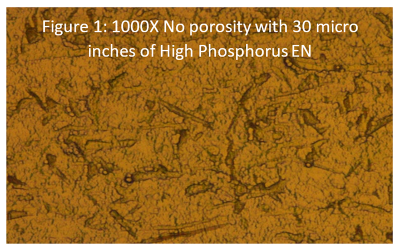
A high phosphorus EN bath further complicates porosity, as high phosphorus EN baths initiate and plate slower and typically require a higher thickness to fill the Pd seed sites. This can be overcome by using organic additives to force more lateral growth, therefore filling the Pd seed sites quicker and at a lower thickness (Figure 1).

What tests have been done to evaluate thin EN deposits?

Figure 2: THP EN passes with lower thickness

There are multiple tests with multiple variations being used in the industry to try to predict how a PCB final finish will perform in the real world. It’s nearly impossible to do every test variation.  The following tests were chosen to evaluate the porosity of different thicknesses of high phosphorus EN. They are listed in order of least to most severe; 

1. 30-minute immersion in 15% nitric with polysulfide indicator
2. 200 Hours 85oC/85% RH
3. Tape test after multiple passes through OSP pre-clean

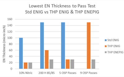
We compared an ENIG with standard EN to a high phosphorus EN in both ENIG & ENEPIG applications. To compare these deposits, figure 2, shows the lowest thickness of each of these 3 deposits needed to pass each test.  Standard ENIG with 150 micro inches could not pass the most difficult test, tape test after 9 OSP passes and needed a higher thickness to pass 15% nitric & 200 hours 85/85. ENIG with THP EN (Thin High Phosphorus Electroless Nickel) was able to pass all tests but required 60 micro inches to pass 200 hours 85/85 and 150 micro inches to pass 9 OSP cycles. ENEPIG with THP EN passes all tests with 30 micro inches of THP EN. THP EN does pass these tests with a lower thickness and can pass the most difficult test, 9 OSP passes, with 30 microinches when used in an ENEPIG deposit.

Performance of THP EN for soldering and gold wire bonding.

Figure 3: THP EN slightly better soldering

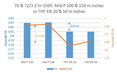
Wetting balance and through-hole soldering were used for comparison of typical EN to THP EN. Through-hole soldering was all 100%, whether THP EN or typical EN, with and without aging. All samples passed wetting balance and the curves all looked very similar. While there is not a lot of difference, even after aging, 20 micro inches of THP EN had a slightly lower time to zero and time to 2/3’s(Figure 3: 0.03 to 0.11 sec). From a solderability standpoint, this all indicates thin deposits of THP EN down to 20 micro-inches solders just as well as 150 micro inches of typical mid phosphorus EN. 

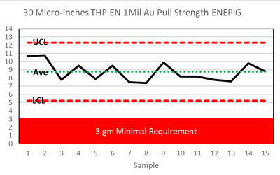
Gold wire bonding was evaluated with 30 micro-inches of THP EN in an ENEPIG deposit.  While the biggest impact to gold bonding is from the pure EP & immersion gold, we wanted to make sure changes in the base metal did not change the ability to gold bond.  Just like soldering, using 30 micro inches of THP EN (Figure 4) performs just a well as 150 micro inches of mid-phosphorus EN.

Figure 4: THP EN Au Wire Bonding @ 30 micro inch
Figure 4: THP EN Au Wire Bonding
@ 30 micro inch


Based on testing, a THP EN deposit provides better protection but with no decrease in solderability and bondability.  Also, testing for insertion loss discussed in an earlier blog “Thin High Phosphorus EN for 5G”2, shows THP EN reduces insertion loss by 50% over typical ENIG deposits. When you step back and look at the entire picture, THP EN with good lateral growth reduces signal loss and provides a deposit with high reliability.  High reliability is certainly required for 5G implementation.

References

1: E Stafstrom, Introduction to D5810, Nov 2020
2: Technic PCB Blog, “Thin High Phosphorus Electroless Nickel for 5G Applications”

Author

Eric%20Stafstrom-150.png

Eric Stafstrom is currently the Global PCB Product Manager at Technic with over 40 years of experience in PCB fabrication and assembly.


Add new comment

Quick Tasks

  • Chemistry
  • Resource Library
  • Useful Tools
  • Industry Partners
  • Contact Us
Back to Top
Corporate Headquarters Technic Inc.
Tel:+1 401-781-6100
Technic Engineered Powders
Tel:+1 401-769-7000
Technic Equipment
Tel:+1 401-721-2300

Contact Us

Locations

  • North America
  • Europe
  • Asia Pacific

Site Footer Menu

  • Applications
    • Semiconductor
    • Components, Lead Frames, Connectors
    • Printed Circuit Boards
    • Industrial
    • Energy Technologies
    • Technic ECO Products
    • Decorative
    • Medical
    • Application Support
  • Chemistry
  • Equipment
    • Automated Systems
    • Manual Lines
    • Laboratory and R&D
    • Anodizing Equipment
    • Parts, Supplies & Accessories
    • Process
  • Engineered Powders
    • Products
    • Global Offices & Distributors
    • Equipment
    • Safety Data Sheets (SDSs)
    • Daily Metal Prices
    • Conflict Minerals Report Request
    • ISO 9001:2015 Certification
    • Contact Us
  • Analytical Controls
    • Capabilities
    • Process Control Products
    • Electrochemical Research Instrumentation
  • About
    • Contact Us
    • News & Events
    • Environmental Stewardship
    • Industry Partners
    • Conflict Minerals Reporting
    • Resources
    • Careers
    • Global Facilities
    • ISO 9001 Registration Certificate
    • Technic SDS Access

Technic Logo in white text

© All Rights Reserved 2024

Footer menu

  • Privacy Policy
  • Legal Information

Follow us online  LinkedIn  Twitter  Facebook

  • Applications
    • Semiconductor
      • Fabrication & Packaging Chemistry
        • Copper
        • Nickel & Tin
        • Precious Metals
        • Photoresist Strippers
        • Metal Etchants
        • Cleaners
      • Analytical Control (RTA)
      • Semiconductor Equipment
        • Semcon 1000
        • Semcon Fountain
        • Semcon 2000
        • Semcon 2500
        • Semcon Wafer Racks
      • High Purity Chemistry
    • Components, Lead Frames, Connectors
      • Electronic Component Chemistry
        • Connectors
          • - Precious Metals
          • - Non-precious Metals
          • - Post-Treatment
        • Lead Frames/LED Substrate Applications
        • Active & Passive Components
      • Electronic Component Finishing Equipment
    • Printed Circuit Boards
      • Chemistry
        • Photoresist Developers, Strippers
        • Preclean and Microetch Products
        • Desmear Chemistry
        • Metallization
        • Copper and Tin Plating
        • Final Finish - Electroplating
        • Final Finishes - Immersion
        • - ENIG
        • - ENEPIG
        • - EPIG
        • - ASIG
      • Imaging Products
        • Photoimageable Materials
          • - TechniFlex LCL
        • IRP Thermosetting Inks
        • Conductive Silver Paste
        • LED Inks
        • Peelable Masks
      • Process Control - EBA
      • Equipment
    • Industrial
      • Pretreatment
        • Cleaners
        • Activators
        • Etchants
      • Electrolytic Plating
        • Nickel
        • Tin
        • Silver
        • Copper
        • Zinc (EU Only)
      • Electroless Plating
      • Immersion
      • Post-Treatment
        • Anti-corrosion/discoloration coating
        • Anti Tarnish
        • Passivation
        • Coatings
        • Strippers
      • Industrial Equipment
      • Anodizing Equipment
    • Energy Technologies
      • Energy Technologies
        • Hydrogen Technology
      • Engineered Powder & Flake
    • Technic ECO Products
    • Decorative
      • Pretreatment
        • Soak Cleaners
        • Electrolytic Cleaners
        • Pickling Solutions
      • Plating Chemistry
        • Gold/Gold Alloy
        • Silver
        • Tin/Tin Alloy
        • White Bronze
        • Nickel/Nickel Alloy
        • Copper
        • Palladium/Palladium Alloy
        • Brass
      • Coatings & Coloring
        • Cataphoretic Lacquers
        • Color Treatments
      • Post-Treatment
      • Glass Etching
      • Equipment
    • Medical
      • Chemistry
      • Equipment
    • Application Support
      • Application Guides
      • Application Notes
  • Chemistry
  • Equipment
    • Automated Systems
      • Hoist Systems
        • Cantilever/Sidearm
        • Rail/Rim Runner
        • Overhead Hoist
        • Hoist Automation
        • Hoist Retrofits
      • Batch Systems
        • Barrels
        • Vibratory
        • SBE Technology
          • - How it works
          • - Configurations
          • - Automation
      • Loose Parts Processing Systems
        • Single Piece (MP500)
        • Single Parts (MP300)
        • Selective Pin (CDP2000)
        • Cut Strip (Leadframes)
        • Panels (MP100)
      • Continuous
        • Reel to Reel
        • Roll-to-Roll (MP200)
      • Turnkey
    • Manual Lines
      • Wet Benches/Modules
      • Tank Lines
    • Laboratory and R&D
      • Mini Lines
      • High Speed Reel to Reel Test Cells
      • Wafer Plating Test Cells
    • Anodizing Equipment
      • Anodizing Mini-Plant
      • Apex Modular Anodizing Equipment
      • Custom Anodizing Equipment
      • Titanium Anodizing Equipment
      • Anodizing Resources
        • What Anodizing System if right for me.
    • Parts, Supplies & Accessories
      • Consoles, Work Stations, Hoods, Benches & Tables
      • Mazerustar Planetary Mixers
        • Demonstration Videos
      • Equipment Support
        • Finishing Equipment Supplier
          • Advanced Engineered Systems
      • Amp Hour Meters, Timers & Chemical Feeders
      • Anodes, Baskets, Bags & Hooks
      • Filtration
      • Precious Metal Recovery
      • Rectifiers
      • Tanks & Auxiliary Equipment
      • Ultrasonic and Aqueous Cleaners & Dryers
      • Selective Plating
    • Process
      • Anodizing
      • Electropolishing
  • Engineered Powders
    • Products
    • Global Offices & Distributors
    • Equipment
      • Conductivity Test Apparatus
        • Tape Application Jig
    • Safety Data Sheets (SDSs)
    • Daily Metal Prices
    • Conflict Minerals Report Request
    • ISO 9001:2015 Certification
    • Contact Us
  • Analytical Controls
    • Capabilities
      • Electroanalytical Methods
      • Data Analysis
      • Volumetric Analysis
    • Process Control Products
      • Real Time Analyzer (RTA)
        • RTA 3D
        • RTA Classic
        • ACE
        • SSF RTA 3D
        • PHD Option
      • EBA
        • EBA 3D
        • EBA 3D: Plus Option
        • EBA Classic
        • Technic Elevate Analyzer
      • Automatic Process Titrator
        • Maestro
        • NextChem Analyzer Support
    • Electrochemical Research Instrumentation
  • About
    • Contact Us
    • News & Events
      • Upcoming Trade Shows
      • Recent Trade Shows
      • Technic Webinars
    • Environmental Stewardship
    • Industry Partners
    • Conflict Minerals Reporting
    • Resources
      • Resource Library
      • Videos
      • Useful Tools
      • Daily Metal Prices
      • FAQ
    • Careers
      • Senior Key Account Manager – Specialty Chemical Semiconductor (Europe)
    • Global Facilities
      • EU Distributors
    • ISO 9001 Registration Certificate
    • Technic SDS Access