
Copper Plating for Advanced Semiconductor Packaging
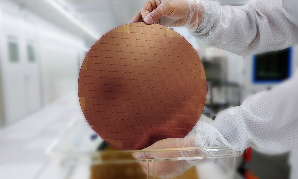 As the semiconductor industry moves to more advanced packaging structures, the use of copper plating has continued to grow. Along with this growth, the requirements on the copper plating solutions and deposit have become more demanding. Technic’s Elevate Copper products are formulated to meet these demanding requirements such as high-speed plating, excellent coplanarity, and very low deposit roughness.
From very tight RDL (redistribution layer) patterns with 2 micron spaces, to 200 micron tall copper pillars, the Elevate Copper processes can be adjusted to offer optimum results on a variety of semiconductor packaging platforms including FOWLP, Fan-In WLP, Flip Chip and 2.5D/3D.
All Elevate Copper processes can be monitored with our industry leading Technic Elevate Analyzer. In addition, we offer unparalleled customer service that has made Technic a respected resource for quality around the globe.
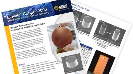
Elevate Cu 3000
Elevate Cu 3000 is a versatile electrolytic copper plating process specifically formulated to plate various types of advanced packaging structures using the same organic system. It can successfully plate RDL patterns, copper pillars, and most other types of features required for advanced packaging. With small adjustments to the operating parameters a flat, convex, or concave feature can be achieved. All organic and inorganic components are fully analyzable with Technic’s Elevate Analyzer.
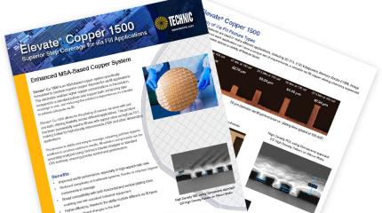
Elevate Cu 1500
Elevate Cu 1500 is an MSA-based copper plating process specially formulated for applications that require excellent via fill and leveling. This product has been successfully used to fill vias with aspect ratios as high as 10:1, making it ideal for high-density interconnects (HDI) and other demanding applications.