
Meeting the Demands of HDI and Ultra HDI
Introduction
Graphite-based direct metallization has advanced to the point where current and future PCB designs depend on efficient, cost-effective, and reliable metallization solutions. This is especially true for HDI and Ultra HDI designs, which require multiple processing steps for each layer:
• Via formation
• Metallization (making holes conductive)
• Imaging
• Electroplating and copper via fill
• Additional finishing steps
• Sequential lamination
Depending on the number of signal and power/ground layers in the stack-up, a design may require several laminations and multiple layers that must be chemically processed. Conventional electroless copper has served the industry well, but alternatives that deliver greater efficiency, reliability, sustainability, and cost-effectiveness deserve serious consideration.
Circudep Black Knight offers compelling advantages in each of these areas.
Advantage #1 – Process Efficiency
Conventional electroless copper requires six to eight chemical steps, with at least one rinse (often two) between each step. For higher-performance laminate materials such as PTFE, polyimide, and flex, additional chemistry is frequently needed to ensure adequate adhesion and coverage.
Black Knight reduces this to just three or four steps. Its highly specialized nano-dispersion of graphite quickly and efficiently coats all resin systems and glass with minimal surface preparation.
Water costs should not be underestimated. Depending on facility location, water can be surprisingly expensive, and in some regions, restrictions have forced fabricators to truck water into their manufacturing sites.
Advantage #2 – Simplicity of Chemistry
There is nothing simpler in this author’s opinion than coating a surface and making it conductive. Electroless copper, by contrast, requires a complex chemical reduction in which copper ions interact with formaldehyde and a palladium catalyst to deposit metallic copper onto the substrate:
2HCHO + 2OH⁻ → H₂(g) + 2CO₂ + 2e⁻
Cu²⁺ + 2e⁻ → Cu (metal)
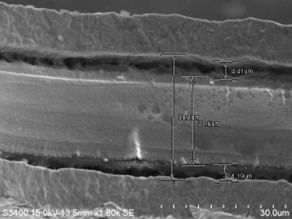
Note the evolution of hydrogen gas during copper deposition. Hydrogen bubbles can become lodged inside vias, potentially causing plating voids (see fig.1).
Black Knight eliminates the need for palladium and avoids creating any intermediate layer between the electrolytic copper deposit and the microvia capture pads or interlayer interconnect. This means a direct bond forms between the electrolytic copper plating and the copper pads, which is a stronger connection than what electroless copper provides. We will explore reliability in greater detail in a future blog.
Advantage #3 – Environmental Savings
With many sequential laminations required for high-density designs, processing each layer through electroless copper—at 45–60 minutes per cycle—is both tedious and resource-intensive. Black Knight requires only 5–6 minutes per cycle, and the difference in water consumption is equally dramatic.
A typical electroless copper line uses 25–30 gallons of rinse water per minute, while Black Knight uses only 5–6 gallons per minute. Combined with Black Knight’s higher throughput, the total water savings are substantial.
Real-World Example: Consider a medium-sized fabricator processing 200 panels per layer per day. With conventional electroless copper, this requires approximately 10–12 hours of processing time. With Black Knight and a horizontal machine processing 40–50 panels per hour, the same volume can be completed in 4–6 hours (fig. 2).
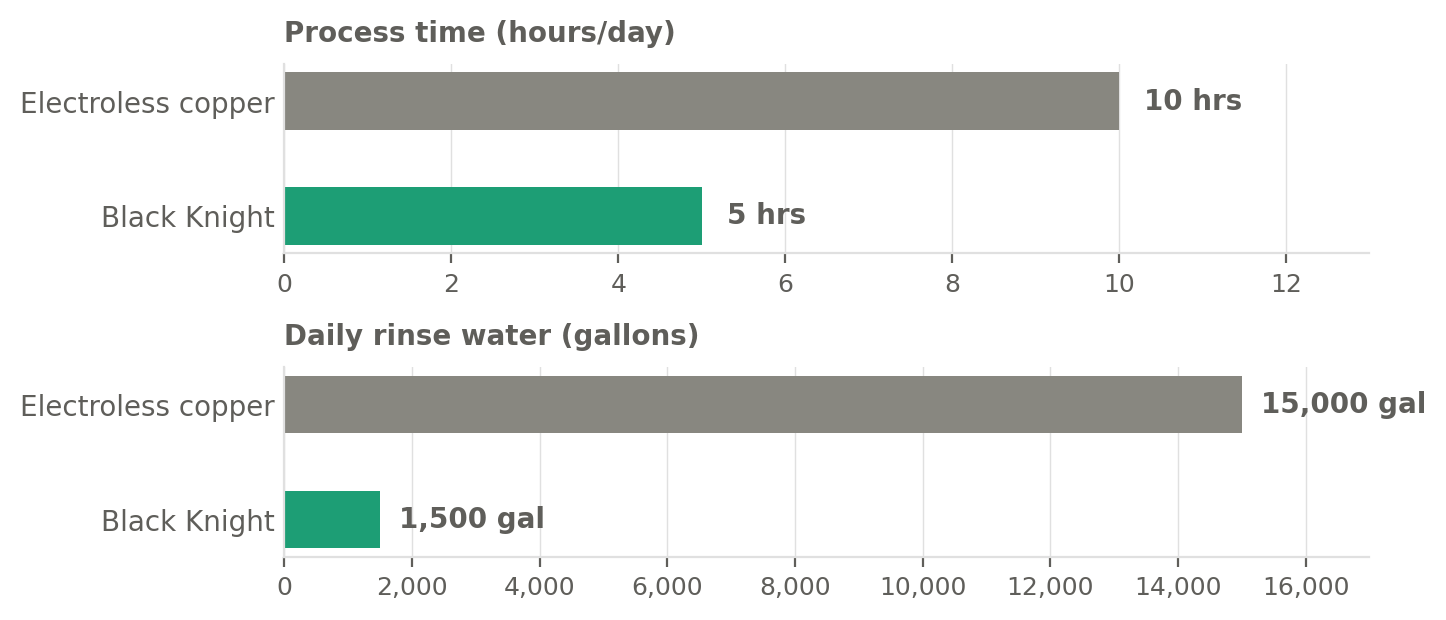
Assuming a five-day work week and 50 operating weeks per year, this amounts to a savings of 67,500 gallons per week and 3,375,000 gallons per year—a figure that is far from trivial.
Advantage #4 – The Science Behind Black Knight
What enables Black Knight to meet the demands of today’s highly complex PCB designs? Beyond process robustness, the answer lies in the chemistry of the system. Specifically, the consistency of the colloidal graphite dispersion and the stability of the colloid.
Consistent Particle Size
Stability in this context has two meanings: the ability to maintain a consistent particle size without aggregation, and the ability of the particles to remain suspended in solution without settling. Each involves different factors.
The Black Knight graphite is a specially formulated hydrophobic colloid, meaning it is not strongly attracted to water. Hydrophobic colloidal particles resist aggregation through two mechanisms: steric repulsion, which creates physical barriers between particles, and electrostatic repulsion, which uses charge to keep particles apart. While both mechanisms contribute to stability, electrostatic repulsion is of particular interest because contaminants can influence the electrostatic charges.
Technic’s team worked diligently to ensure that the nano-dispersion maintains consistent particle size and conductivity throughout extended processing runs, meaning fabricators can expect uniform metallization and reliable results from the first panel to the last.
Crystalline Structure and Conductivity
Unlike carbon black, which is amorphous, Black Knight graphite occurs as a highly crystalline substance. Its hexagonal lattice forms a honeycombed arrangement of carbon atoms that promotes anisotropy, which is the property of being directionally dependent. An isotropic material, by contrast, has identical properties in all directions.
For through-hole and blind via plating, this anisotropy is a key advantage: the graphite is highly electrically conductive, making it well suited for metallization. When resistance through a plated through-hole or blind via is low, electroplating of copper proceeds at a faster rate, with enhanced throwing power, resulting in more uniform copper distribution and fewer plating defects. This is a distinct feature of the Black Knight process.
Summary
The versatility and performance advantages of Black Knight are well documented. Its ability to metallize a wide array of laminate and resin materials makes it the go-to process for difficult-to-metallize substrates, while its streamlined chemistry delivers considerable gains in throughput, cost-effectiveness, and process reliability. At the same time, the measurable savings in water and electricity consumption deserve serious consideration in any PCB fabrication operation.
Let the Technic team help you reduce costs, improve reliability, and maximize the efficiency of your operation.
Author
.jpg) Mike Carano, PWB Final Finishes Consultant
Mike Carano, PWB Final Finishes Consultant
References
"Alternative Technologies for Making Holes Conductive” https://www.epa.gov/sites/default/files/2013-12/documents/pwb_mhc_alternatives.pdf
https://iconnect007.com/article/146908/trouble-in-your-tank-implementing-direct-metallization-in-advanced-substrate-packaging/146905/pcb
Aggiungi un commento