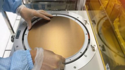
Advanced Solutions for Semiconductor Manufacturing
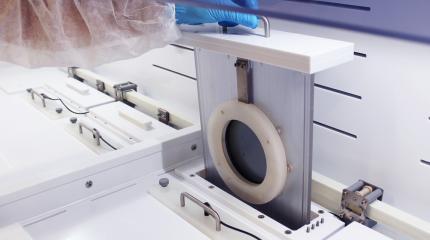
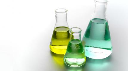
Technic supplies some of the most advanced solutions for semiconductor fabrication and packaging in the industry including electroplating chemistry, photoresist strippers, cleaners (post etch residue removers), metal etchants, and high purity wet chemistry, as well as semiconductor manufacturing equipment.
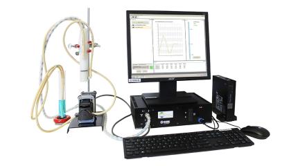
High-performance product development, with application specific characteristics and unparalleled analytical expertise, provides customers with the essential tools to meet the challenges of today’s semiconductor manufacturing.